Published: March 2026
To improve accessibility, the report text has been reproduced below.
The advanced vacuum component sector enters 2026 at a pivotal moment.
Demand for high-reliability ceramic-to-metal components, hermetic feedthroughs, and ultra-high vacuum (UHV) assemblies continues to rise – especially across the aerospace, defense, semiconductor manufacturing, medical imaging, photonics, and advanced energy sectors. Market research firms project a 5%+ compound annual growth rate (CAGR) through 2032, driven by increasing demand in the above industries and continued technological advancements that increasingly depend on hermeticity, dependability in extreme environments, and device miniaturization.
Performance expectations once reserved for defense or experimental systems are becoming baseline requirements across commercial applications. Downtime, contamination, and requalification now carry costs measured in millions of dollars per event, pushing OEMs to demand greater reliability at the component level.
Several macro trends are converging to shape demand in 2026 and beyond. Capital investment in semiconductor fabrication, laser and photonics systems, and space platforms remains strong. Energy sector innovation – particularly in fusion research and cryogenic systems – is introducing new requirements for sealing performance under extreme thermal and pressure conditions.
These trends have been anchored by large, visible programs. Multi-billion-dollar semiconductor fabrication plants announced under the CHIPS and Science Act (e.g. facilities from Intel, TSMC, Samsung, and Micron) are locking in long-term demand for physical vapor deposition, chemical vapor deposition, atomic layer deposition, and extreme ultraviolet lithography tools. Each depends on UHV-grade feedthroughs, viewports, and sensor penetrations. Private fusion companies have collectively raised over $7.1 billion to advance pilot plants and demonstration devices, requiring radiation-tolerant, cryogenic-capable ceramic-to-metal assemblies.
As these forces collide, the advanced vacuum sector is moving toward vertically integrated manufacturing partners with deep engineering expertise, in-house testing capabilities, and the technical expertise necessary to support custom designs from concept through scaled production.
Success in the coming years will increasingly depend on collaboration, qualification speed, and component reliability – not simply catalog availability.
By the end of 2025, the vacuum component market reflected steady growth paired with rising complexity. Ceramic-to-metal sealing technologies have evolved from niche research components to foundational elements in systems where vacuum integrity, electrical isolation, thermal stability, and long service life are essential.
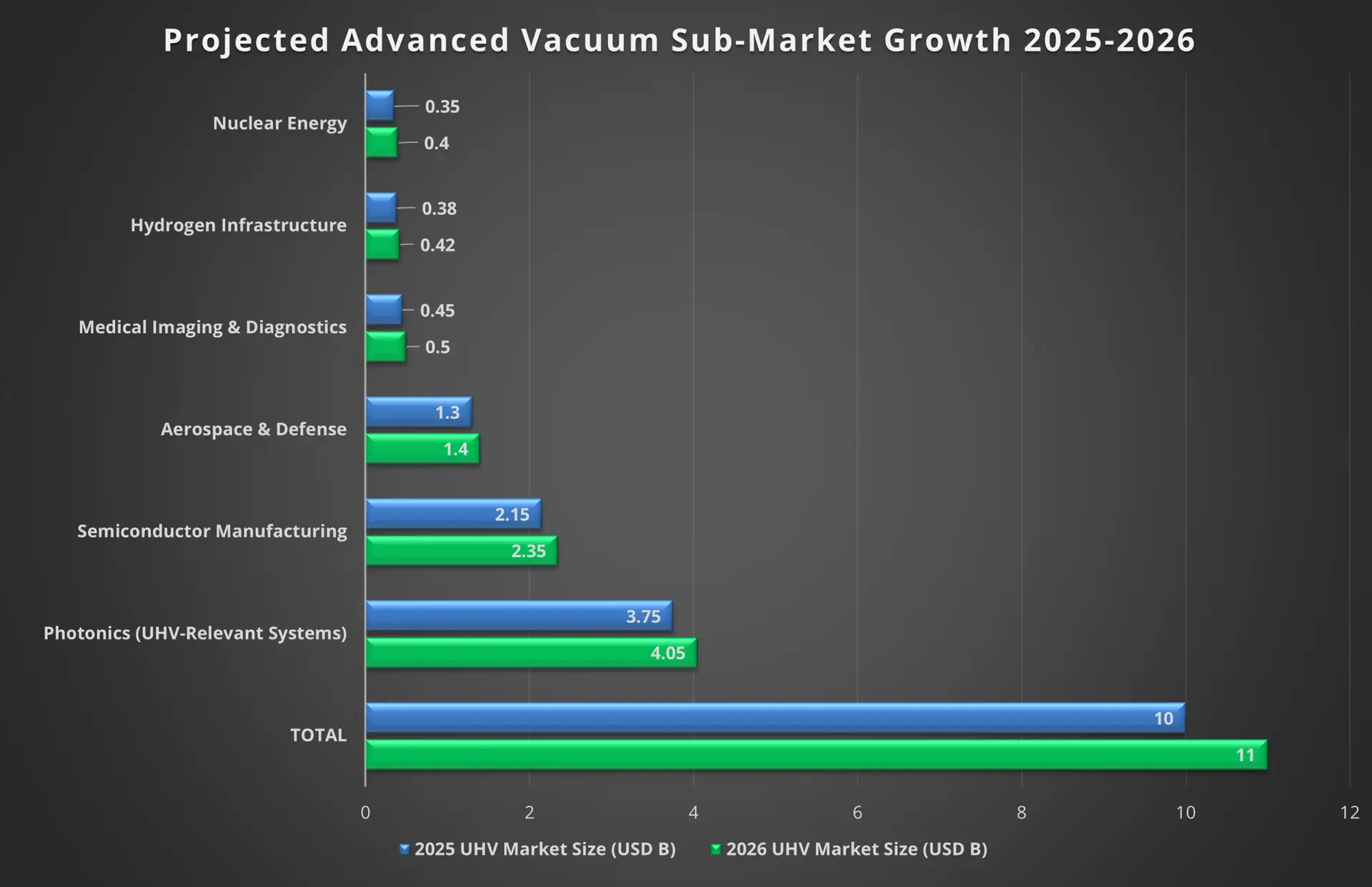
Demand was driven primarily by five sectors: aerospace and defense programs, semiconductor manufacturing and vacuum coating systems, medical imaging and diagnostic equipment, photonics and laser platforms, and energy research. Each placed increasing emphasis on performance under extreme conditions, repeatability across production runs, and rigorous validation through testing and documentation.
In 2025, these requirements became routine expectations in mainstream capital equipment. Semiconductor fabrication expansion under national industrial-policy initiatives, medical OEMs pushing toward higher-resolution imaging systems, and defense programs fielding sophisticated sensing and directed-energy platforms all converged on similar demands: lower acceptable leak rates, tighter control of outgassing and contamination, and stronger documentation around materials and process histories.
Manufacturers also faced mounting operational constraints in 2025. Global supply chains remained fragile following years of disruption, and tariff volatility continued to influence sourcing for raw materials and subcomponents. Lead times for specialty metals, ceramics, and brazing alloys fluctuated greatly, forcing vendors and OEMs to place greater value on suppliers with domestic manufacturing capacity and inventory control.
By the close of 2025, many OEMs had consolidated portions of their supplier base around fewer manufacturing partners who could best navigate rapidly evolving market conditions and support co-design, rapid prototyping, and in-house validation testing to reduce hand-offs and suppress lead times.
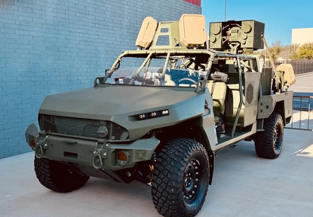
Aerospace and defense remain among the strongest drivers of UHV component demand entering 2026. Space commercialization continues to accelerate across satellite deployments, ground-based infrastructure, and an emerging tourism market — much of which requires components capable of withstanding radiation exposure, wide thermal cycling, and prolonged vacuum operation without degradation.
Defense applications introduce additional performance demands. Directed energy systems, advanced sensing platforms, and high-energy optics impose stringent requirements on sealing performance, electromagnetic compatibility, and structural stability. Failure tolerance in these applications is exceptionally low, making ceramic-to-metal assemblies that offer consistency across extreme conditions an increasingly critical specification.
The integration of precision optics into both space and defense platforms has further elevated expectations. Boundary-pushing applications are driving demand for components that combine vacuum and optical functionality, positioning single-source providers for meaningful competitive advantage — particularly in laser- and sensor-driven systems.
This trajectory is reinforced by defense modernization and space-asset resilience initiatives, which are pushing platforms into persistent, long-duration operational roles. Laser communication terminals, high-resolution imaging payloads, and space-based sensing constellations all depend on vacuum-compatible optical and electrical interfaces that can perform without maintenance across deployments spanning years. As these platforms proliferate, vacuum components are increasingly specified not just for initial performance, but for documented, end-to-end reliability across the full mission profile.
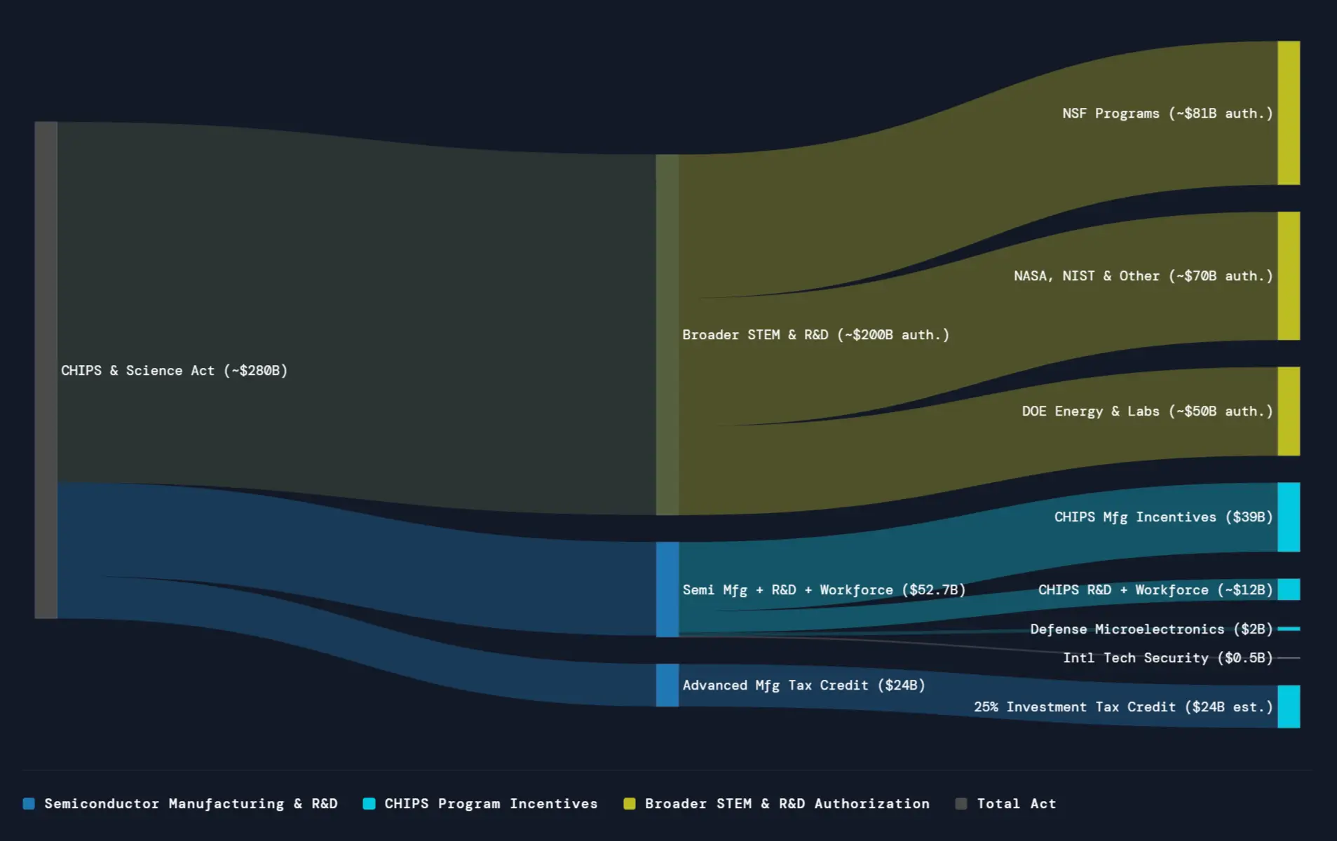
Semiconductor manufacturing continues to expand at a historic pace, driven by global investment in advanced fabrication facilities, packaging innovation, and supply chain localization. The CHIPS and Science Act committed $39 billion toward domestic semiconductor manufacturing, with over $32 billion allocated to 31 companies across 48 projects in 23 states as of January 2025. Major players including Intel, TSMC, Samsung, and Micron have announced multi-billion-dollar semiconductor fabrication plant projects across North America, Europe, and Asia.
Modern semiconductor fabrication relies extensively on ultra-high vacuum conditions across multiple process steps, including physical vapor deposition (PVD), chemical vapor deposition (CVD), atomic layer deposition (ALD), etching, and ion implantation. Tool manufacturers such as Applied Materials, Lam Research, KLA, and ASML build systems that rely on stable vacuum boundaries to maintain process precision at the nanometer scale.
In advanced nodes below 5 nm, even minor contamination events can result in yield loss worth millions of dollars per production run.
National industrial-policy incentives and private capital are translating into concrete capacity additions. New and expanded facilities represent multi-billion-dollar commitments, each embedding fleets of deposition, etch, lithography, and metrology tools. Every tool incorporates dozens to hundreds of vacuum penetrations (electrical, optical, and thermal) that must meet stringent leak-rate and outgassing specifications over long service lives.
ASML’s EUV lithography systems exemplify this trend. After a decade of R&D, ASML shipped its first High NA EUV lithography modules to Intel in December 2023, with each unit costing approximately $370 million. The company has capacity to produce five to six High NA EUV systems annually and holds orders for 10 to 20 machines.
The continued expansion of AI infrastructure further amplifies this trend. Advanced GPUs and AI accelerators require leading-edge fabrication nodes and high-density packaging technologies, increasing the technical burden on vacuum-dependent fabrication equipment. As semiconductor capital expenditures remain elevated and fabrication complexity continues to grow, demand for precision, hermetically sealed, UHV-rated components is expected to remain strong through 2026 and beyond.
Medical imaging, diagnostics, and therapeutic systems place increasingly sophisticated demands on UHV sector manufacturers. Many advanced diagnostic and therapeutic platforms rely on vacuum-stable environments and hermetically sealed electrical penetrations to operate reliably.
In imaging systems such as CT scanners, PET systems, and advanced X-ray tube assemblies, vacuum integrity is essential to accelerate electrons and maintain a stable beam. Even minor leakage or contamination can degrade imaging performance, reduce tube life, or require costly system downtime. As imaging resolution improves and systems become more compact, feedthroughs and sealed interfaces must maintain electrical isolation and structural stability within increasingly constrained geometries.
Miniaturization trends are pronounced in emerging applications including compact diagnostic imaging units for outpatient and mobile care environments, proton therapy and targeted radiation delivery systems, and cryo-electron microscopy (cryo- EM) platforms used in pharmaceutical research. The global proton therapy market is projected to grow from $1.57 billion in 2023 to $5.86 billion by 2032 (15.8% CAGR), while the cryo-EM market is expected to nearly triple from $1.45 billion in 2025 to $3.18 billion by 2032, driven by demand from pharmaceutical R&D programs.
In these systems, space constraints introduce complex engineering challenges. High-density feedthroughs must transmit power, signal, or thermal data across a vacuum boundary without compromising isolation or increasing outgassing risk. Reduced physical size often increases thermal density, elevating mechanical stress at the ceramic-to-metal interface. Managing coefficient-of-thermal-expansion (CTE) mismatches and maintaining seal integrity over extended thermal cycling becomes increasingly critical as devices miniaturize.
Cryogenic operation adds another layer of complexity. Cryo-EM systems and certain advanced imaging technologies require stable operation at extremely low temperatures to reduce thermal noise and improve resolution. Components supporting these systems must tolerate repeated cycling between ambient and cryogenic conditions without microfracturing or seal degradation.
Beyond performance considerations, regulatory requirements intensify the engineering challenge. Medical devices must demonstrate consistent performance across long service lifetimes, often under FDA or equivalent international regulatory oversight. Hermetic sealing solutions must meet vacuum and thermal performance benchmarks as well as biocompatibility standards, sterilization durability, and traceability documentation requirements.
These regulatory expectations are especially pronounced for Class II and Class III devices and for implant-adjacent electronics, where service lives can extend well beyond a decade. As healthcare providers continue to adopt higher-resolution imaging, targeted therapies, and portable diagnostic platforms, manufacturers that can align engineering, documentation, and quality systems with these expectations will capture a growing share of vacuum-related medical demand.
Photonics and laser-based systems are among the fastest-growing demand drivers for precision UHV components, expanding across industrial manufacturing, semiconductor fabrication, defense, and aerospace at a sustained pace. The global industrial laser market was valued at approximately $23.6 billion in 2024 and is projected to nearly double to $48 billion by 2033, growing at a 9.2% CAGR, driven by high-power cutting, welding, and additive manufacturing applications.10 The broader photonics market – encompassing optical sensors, laser sources, and beam delivery systems – exceeded $979 billion in 2024 and is forecast to reach $1.3 trillion by 2030. Across these platforms, tightly controlled vacuum environments are foundational: contamination, thermal distortion, or seal degradation can directly degrade beam quality, reduce system life, or cause catastrophic optical damage.
In semiconductor manufacturing, EUV lithography systems depend entirely on high-vacuum environments along the entire optical path from source to wafer, with residual gas composition tightly controlled to protect mirror reflectivity. On the defense side, high-energy laser systems for directed-energy applications exceeded $10.3 billion in market value in 2024, growing at 8.2% CAGR through 2034, driven by military investment in counter-drone and missile defense programs. These platforms, along with space-based laser communication terminals and advanced imaging payloads, rely on UHV-compatible optical windows and feedthroughs to maintain performance over multi-year operational missions without access for maintenance or requalification.
The engineering demands at these energy densities are severe. Localized heating at high repetition rates or sustained power levels creates mechanical stress at the ceramic-to-metal interface. The integration of advanced optical coatings (anti-reflective, high-reflectivity, or wavelength-specific) adds further complexity. These coatings must adhere reliably to substrates that may experience vacuum cycling, plasma exposure, and mechanical stress, requiring close alignment between optical fabrication and hermetic sealing processes to preserve both optical performance and structural integrity simultaneously.
As photonics and laser systems transition from research and prototype environments into scaled production and operational deployment, expectations for qualification documentation, manufacturing repeatability, and production scalability are rising accordingly. OEMs are increasingly seeking partners capable of delivering integrated optical and ceramic-to-metal assemblies that can be validated, reproduced, and scaled alongside evolving, and advancing, platform requirements.
Quantum computing is emerging as a strategically significant growth area for ultra-high vacuum systems and precision hermetic components. While at varying stages of commercialization depending on architecture (superconducting qubits, trapped ions, neutral atoms, photonic systems), most leading quantum computing platforms rely on tightly controlled vacuum environments and extreme thermal stability to operate reliably.
Superconducting-qubit platforms developed by major technology companies and research consortia typically stack multiple temperature stages from room temperature down to a few millikelvin. Hermetic feedthroughs and sensor penetrations in these systems must maintain integrity and low outgassing while enduring repeated thermal cycles across this full range. Trapped-ion and neutral-atom architectures place a premium on achieving extreme-high-vacuum conditions, where even trace residual gases can limit coherence times and gate fidelities. Photonic quantum platforms emphasize low-loss optical interfaces, stable packaging, and long-term alignment.
As quantum systems scale from laboratory prototypes to commercially viable architectures, component reliability becomes increasingly critical. Feedthroughs, viewports, and sealed assemblies must support ultra-low leak rates (often 10-¹¹ cc/sec or lower), thermal cycling across cryogenic ranges, and electromagnetic stability.
Public and private investment into quantum hardware has risen steadily, particularly for trapped-ion and photonic systems that promise clearer scaling paths. As more hardware moves into cloud-accessible quantum services and early commercial deployments, expectations for documentation, qualification testing, and serviceability are converging with those seen in semiconductor and high-reliability defense equipment.
While the quantum market remains smaller than aerospace or semiconductor sectors, its technical requirements are among the most stringent in modern manufacturing. This makes it a high-impact vertical for precision ceramic-to-metal and hermetic sealing technologies.

Energy innovation is reshaping the vacuum component landscape beyond traditional industrial applications. Nuclear fission is experiencing renewed strategic investment, particularly as global energy demand rises alongside rapid expansion of data centers, AI infrastructure, and electrified transportation. Advanced reactor designs – including small modular reactors (SMRs) and next-generation fission platforms – emphasize improved safety, modularity, and efficiency, placing new performance expectations on components used in instrumentation and control systems.
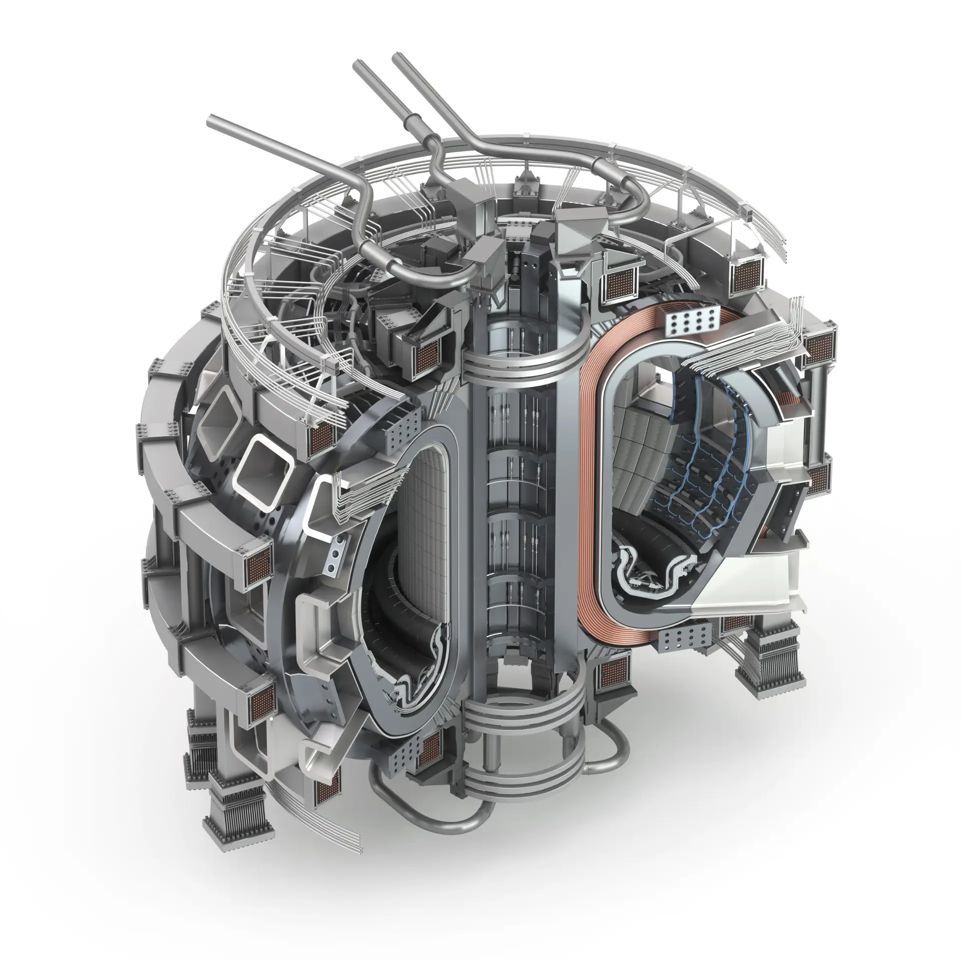
Fusion research is among the most technically demanding emerging sectors for UHV component manufacturers. Major international programs such as ITER, along with privately funded ventures including Commonwealth Fusion Systems (which raised $2.1 billion), Helion Energy (which secured over $1 billion and is constructing its Orion pilot plant in Washington State), and TAE Technologies, are pursuing commercially viable fusion architectures. The global fusion hardware, equipment, and technology market is projected to grow from approximately $344 million in 2025 to over $533 million by 2032.
These systems operate under conditions combining extreme vacuum, intense magnetic confinement, neutron flux, cryogenic cooling, and high thermal loads. In magnetic confinement fusion systems, plasma chambers must maintain ultra-high vacuum conditions to sustain stable plasma behavior. Diagnostic instrumentation, magnetic coils, and plasma-facing components require electrical and optical feedthroughs that operate reliably in high-radiation and high-temperature environments. Cryogenic systems are frequently used to cool superconducting magnets, introducing repeated thermal cycling between ambient and cryogenic conditions. These combined stresses demand ceramic-to-metal seals that can tolerate extreme CTE mismatches without degradation.
Private fusion companies are now designing and constructing pilot plants and large experimental devices rather than only small-scale test rigs. These platforms can incorporate thousands of individual penetrations for power, sensing, cooling, and safety systems, many of which must withstand a mix of vacuum, high pressure, cryogenic temperatures, and radiation. As timelines compress and investors focus on demonstrable progress toward grid-connected systems, UHV and hermetic components that can be qualified quickly and perform reliably under combined stressors become critical enablers.
Beyond fusion, hydrogen production and storage technologies contribute to increased demand for robust hermetic sealing. Electrolyzers, hydrogen transport systems, and cryogenic storage tanks introduce combinations of pressure differentials, thermal cycling, and reactive gas exposure that challenge conventional sealing approaches. Similarly, advanced energy storage and high-voltage transmission systems rely on vacuum interrupters and sealed assemblies to maintain reliability under load.
Unlike many legacy industrial systems, emerging energy platforms often operate under multiple extreme conditions simultaneously. This convergence increases the importance of precision engineering, validated leak-rate performance, and material compatibility under dynamic mechanical stress.
Historically, components rated for extreme temperature and pressure ranges were reserved for specialized aerospace, defense, or research programs. In 2026, that distinction is fading. Fusion pilot plants now routinely specify feedthroughs that cycle from below 4 K (superconducting magnet cooling) to 400–600°C bake-out temperatures, while hydrogen systems must simultaneously manage 30,000+ PSI pressures and −253°C cryogenic conditions.
Meeting these combined requirements demands materials and joint designs that control CTE mismatches across the full envelope, plus in-house test stands capable of replicating the complete mission profile (e.g. 500+ cryo cycles, 10,000+ hours of high-temperature operation). These examples illustrate a broader shift: extreme performance envelopes are becoming baseline engineering requirements across multiple sectors.
As failure tolerance decreases and system complexity increases, manufacturers must adjust accordingly. Advanced and efficient in-house testing infrastructures – encompassing the various stress modalities mentioned – will increasingly differentiate suppliers, particularly in markets where qualification cycles are long and failure costs are high.
Leak-rate benchmarks continue to tighten across industries as system sensitivity increases and the cost of contamination rises. Helium leak rates of 10⁻⁹ cc/sec have become widely accepted baseline requirements for many UHV applications. This corresponds to roughly one cubic centimeter of helium (the smallest atom) escaping over several decades of continuous operation. However, in the most demanding environments, acceptable leak rates extend to the 10⁻¹⁰ to 10⁻¹¹ cc/sec range.
These tightened thresholds reflect application-specific physics:
Across these platforms, even 10⁻⁹ cc/sec leakage introduces residual gases that shorten coherence times, trigger yield excursions, or force recalibration cycles costing days of downtime. The shift toward ever more stringent leak thresholds reflects a broader redefinition of reliability. What was once considered exceptional performance is now becoming standard in advanced research and high-value commercial systems.
Consistently achieving and verifying leak rates in the 10⁻¹⁰ to 10⁻¹¹ range requires advanced helium mass spectrometry, rigorous calibration protocols, clean assembly environments, and documented quality control processes. Manufacturers with in-house leak-detection infrastructure capable of meeting these thresholds will be better positioned to support next-generation aerospace, semiconductor, quantum, and energy platforms.
Advances in metallization and joining technologies continue to expand what is possible in ceramic‑to‑metal assemblies, particularly as operating environments grow more extreme and component geometries more complex. As applications push toward simultaneous cryogenic and elevated‑temperature conditions, sealing strategies are evolving beyond simple CTE “matching” into more deliberate management of thermal strain across the joint, with new methods and process controls aimed at keeping residual stress within safe limits over long service lives.
Active metal brazing has gained increased adoption in advanced ceramic-to-metal joining applications where direct bonding eliminates the need for separate metallization and plating steps. By consolidating these operations into a single joining cycle, this method reduces process interfaces and shortens overall production time. The incorporation of reactive elements promotes direct chemical interaction with ceramic substrates, enabling strong interfacial bonding, improved wetting behavior, and the potential for more compact joint configurations.
Molybdenum-manganese (Mo-Mn) thick-film metallization remains a foundational approach for high-reliability ceramic joining due to its interface stability and process predictability. The pre-applied metallized layer enhances braze wetting control, improves joint-to-joint consistency, and reduces variability associated with direct ceramic reactions. This controlled interface architecture contributes to repeatable hermetic sealing and improved resistance to thermal cycling stresses in demanding applications.
Advancements in furnace technology and process monitoring have further elevated joining reliability, with improved atmosphere control, tighter temperature uniformity, and enhanced ramp‑rate precision. This allows manufacturers to better manage thermal gradients during brazing cycles. Modern vacuum and induction brazing lines emphasize parts‑per‑billion atmospheric purity and ramp rates held to approximately 1°C/min, supported by real‑time observation of braze flow and gap closure to reduce internal stress formation, minimize distortion in large assemblies, and improve repeatability across production batches. These techniques are being pushed to meet increasingly demanding leak‑rate thresholds for quantum, fusion, and space applications, making process control at the microstructural level as important as the choice of filler alloy itself.
Materials science developments are enabling improved braze alloys and refined metallization chemistries that better accommodate CTE mismatches between ceramics and metals, a critical factor for assemblies exposed to repeated temperature cycling. Emerging work on tailored glass‑ceramic and active braze systems, combined with digital tools that model thermal strain and joint behavior, reflects a broader shift toward treating the seal as an engineered interface rather than a static material pair.
For customers migrating legacy Kovar/glass designs to ceramic‑to‑metal in high‑value quantum and fusion programs, the ability to validate these controls through cross‑section analysis, accelerated lifecycle testing, and documented process discipline often becomes the deciding factor in supplier selection.
Digital tools are fundamentally reshaping how high-reliability UHV components are designed and qualified. SolidWorks modeling combined with finite element analysis (FEA) is now a baseline expectation, but engineering workflows have advanced well beyond structural modeling. Modern multiphysics simulation platforms evaluate thermal gradients, mechanical stress, electrical field distributions, and vacuum behavior within a single integrated environment, allowing engineers to assess CTE behavior, outgassing risk, and electromagnetic compatibility virtually, before committing to physical prototypes. The business case is well established: simulation-led design has been shown to reduce development costs by approximately 20% while compressing time-to-qualification.
Generative design tools, computational fluid dynamics (CFD) modeling for vacuum and gas-flow behavior, and digital twin frameworks are extending these capabilities further. Digital twins are particularly impactful in high-volume semiconductor fabrication environments, where real-time sensor data feeds back into virtual models to refine predictions of thermal fatigue, leak-rate drift, and process variation over time.
Artificial intelligence is accelerating this further. AI-driven surrogate models can predict residual stress evolution in complex brazed assemblies significantly faster than full multiphysics simulation, enabling design teams to iterate across dozens of braze-alloy and geometry combinations before cutting metal. For quantum and fusion customers migrating legacy Kovar/glass designs to ceramic-to-metal, this kind of rapid virtual iteration, backed by cross-section analysis and accelerated lifecycle testing, meaningfully compresses the qualification timeline.
Predictive engineering will not replace physical testing, particularly in heavily regulated or mission-critical applications where documented validation is required. What it will do is shift where validation effort is concentrated, narrowing the range of physical prototypes needed and identifying design vulnerabilities earlier in the process. Manufacturers who combine advanced simulation capability with in-house test infrastructure are best positioned to shorten development cycles, reduce iterative redesign, and give OEM partners greater confidence before committing to full production.
OEMs across aerospace, semiconductor, energy, and photonics sectors are consolidating supplier bases and favoring partners capable of delivering design, manufacturing, and testing under one roof. This trend reflects both economic and operational realities: as systems grow more complex and qualification cycles more expensive, every additional vendor interface or handoff introduces potential risk—dimensional drift, documentation gaps, communication delays, misaligned quality standards, and extended lead times.
Vertically integrated vacuum component manufacturers can instead deliver fully finished assemblies – complete with integrated optics, wiring harnesses, and instrumentation, leak tested and ready for chamber integration, which eliminates weeks of line-side assembly risk for semiconductor toolmakers and simplifies ITAR-controlled qualification for defense OEMs.
Shorter product development cycles, particularly in AI-driven semiconductor infrastructure and emerging energy technologies, further favor manufacturers able to iterate rapidly without dependence on external vendors for subcomponents, testing, or validation. As qualification standards tighten, vertically integrated suppliers controlling design, production, and testing internally are positioned to gain durable competitive advantage over those reliant on fragmented outsourcing models.
Geopolitical dynamics are increasingly influencing sourcing decisions across vacuum-reliant industries. China remains a significant global player in vacuum technology and advanced materials manufacturing, and many vacuum components, ceramics, and specialty metal assemblies have historically been sourced from international suppliers. However, rising geopolitical tensions, export controls, and national security considerations are prompting renewed scrutiny of global supply chains.
In the United States, policies such as the CHIPS and Science Act and broader industrial policy initiatives have emphasized domestic manufacturing resilience in semiconductor and advanced technology sectors. The CHIPS Act explicitly prohibits funding recipients from expanding semiconductor manufacturing in China or countries deemed national security threats, effectively requiring domestic supply chain alignment as a condition of participation in federally supported fabrication programs.
The Department of Commerce’s Bureau of Industry and Security (BIS) has further tightened this environment through a series of export control updates in 2022, 2023, and 2024, progressively restricting the export of advanced semiconductor manufacturing equipment and related technologies. December 2024 rules extended Foreign Direct Product controls to cover equipment and components produced outside the U.S. using American technology. For UHV components embedded in EUV lithography tools, advanced-node fabs, and AI accelerator production lines, these controls create a strong and growing preference for fully domestic supply chains.
Quantum hardware and fusion pilot plants face similar pressures from a different direction. A draft executive order circulating in early February 2026 would direct the Departments of Energy, Defense, and Commerce to align manufacturing infrastructure and supply chain strategy with national quantum priorities, and explicitly emphasize counterintelligence protections and domestic manufacturing capacity as conditions for federal support. Defense and ITAR-adjacent programs continue to enforce domestic sourcing requirements under Buy American provisions, which require that 65% of defense procurement value originate domestically as of 2024, rising to 75% by 2029.
Full reshoring is neither immediate nor universal. Many industries continue to rely on international partners for raw materials, specialty ceramics, and niche fabrication capabilities. The likely trajectory is not wholesale decoupling, but rather strategic realignment and selective localization of high-risk components.
As geopolitical uncertainty persists, manufacturers with secure domestic operations, transparent supply chains, and compliance-ready infrastructure are positioned to benefit. Suppliers heavily reliant on single-region offshore production may face increased scrutiny or risk exposure as OEMs rebalance sourcing strategies.
Specialized manufacturing in the vacuum sector depends on highly skilled engineers, technicians, machinists, brazing specialists, and quality inspectors. Over the past several years, labor market conditions have fluctuated significantly. While certain advanced manufacturing segments previously experienced tight labor conditions, broader macroeconomic shifts have resulted in a more balanced labor market entering 2026.
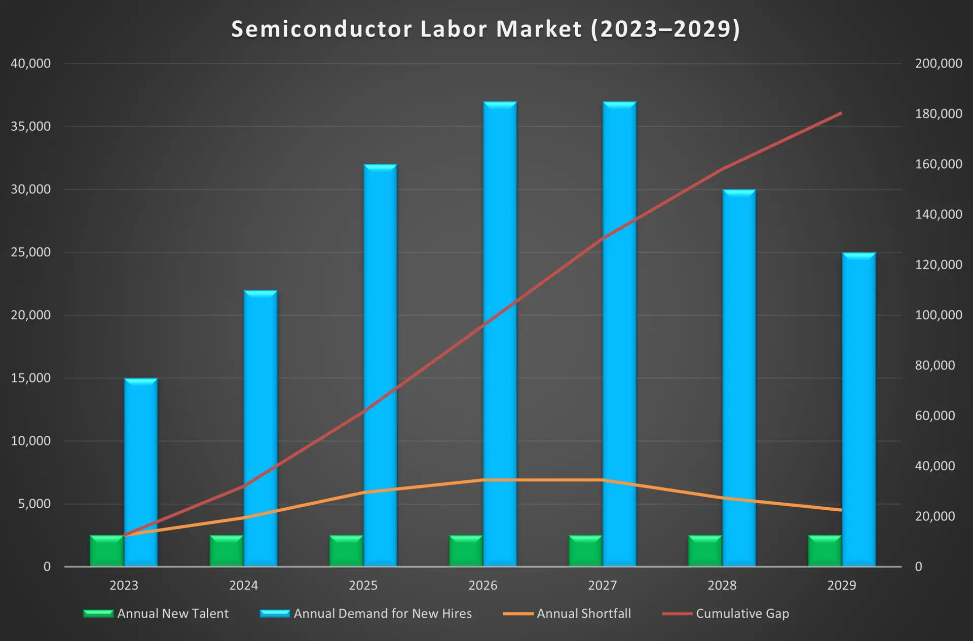
Advanced manufacturing sector turnover reached 27.5% in 2024, meaning employers replaced nearly a third of their workforce in a single year. McKinsey projects a potential gap of approximately 59,000 engineers and technicians in semiconductor manufacturing alone by 2030, even if CHIPS Act-funded training programs hit their stated targets. The skilled trades most critical to high-reliability vacuum component production require years to master, and seasoned workers are retiring faster than the pipeline can replace them.
Demographic pressure compounds this challenge. Of the roughly 3 million U.S. manufacturing workers aged 55–64, a large share will exit the workforce over the coming decade, taking with them institutional knowledge and process discipline that cannot be quickly rebuilt.
For advanced vacuum component manufacturers, this is particularly consequential: the process judgment embedded in a skilled brazing technician or leak-test specialist represents a competitive asset that cannot be transferred through documentation alone.
A loosening labor environment may present an opportunity for manufacturers seeking to strengthen internal capabilities. Companies prioritizing investment in advanced testing infrastructure, simulation engineering, and quality control systems may find it more feasible to recruit experienced technical talent than during prior peak hiring cycles.
As UHV applications expand into increasingly complex sectors such as fusion, quantum computing, and advanced semiconductor fabrication, engineering sophistication will be as important as production capacity.
As digital design tools, advanced simulation platforms, and AI-assisted generative design mature, OEMs are increasingly able to move from performance targets directly to custom-engineered components, rather than constraining system architectures to fit existing catalog parts.
In semiconductor fabrication, toolmakers continuously refine chamber geometries to support advancing chip manufacturing processes. In energy and aerospace, custom configurations are often required to accommodate extreme thermal gradients or pressure loads that no standard catalog component was designed to survive.
As the economic penalty for performance compromise grows – particularly in high-capital, low-tolerance applications – the value proposition of custom-capable manufacturers over catalog suppliers strengthens accordingly.
Global investment in laser and photonics systems continues to expand across industrial, defense, and semiconductor applications, driven by AI infrastructure, LiDAR, precision manufacturing, directed energy, and satellite communication platforms.
ASML’s ~$370 million EUV lithography systems represent some of the most demanding vacuum-optical integrations in commercial manufacturing, with system shipments continuing to grow as advanced-node capacity expands.
On the defense side, the U.S. Army and Navy are actively field-testing directed-energy demonstrators that require UHV-rated windows and beam-transport assemblies capable of sustaining kilowatt-level flux over operational duty cycles.
As these platforms transition from demonstrators to fielded systems, demand for production-qualified UHV optical assemblies will grow in both volume and technical stringency.
Performance expectations once confined to defense and space programs are now shaping commercial systems as the cost of failure has risen sharply across multiple industries.
In data centers, the Uptime Institute’s 2025 outage analysis found that 20% of significant outages in 2024 exceeded $1 million in total cost driven by the increasingly critical nature of digital infrastructure and rising recovery complexity. Similarly, advanced semiconductor manufacturers face yield loss exposure worth millions of dollars per contamination event.
In both environments, leak-rate thresholds, documentation rigor, and lifecycle validation requirements are tightening to levels that previously characterized only defense procurement. Simultaneously, dual-use technology classification and tightening export controls are further blurring the boundary between commercial and defense-grade engineering standards. This general trend is expected to continue.
As fusion pilots advance, hydrogen infrastructure scales, and next-generation aerospace propulsion evolves, demand for seals capable of tolerating simultaneous cryogenic and elevated-temperature operating conditions will intensify.
Global private investment in fusion reached $2.64 billion in the twelve months leading to July 2025, which is the second-highest annual figure on record. 84% of responding fusion companies project grid-connected electricity delivery before 2040.
Advanced braze alloys, refined metallization chemistries, and improved furnace process control are enabling better management of thermal stress and fatigue under cyclic loading across these demanding programs. These are not temporary research anomalies – they represent a structural shift in engineering demand that will persist well beyond 2026.
For manufacturers with validated extreme-environment sealing capability and the testing infrastructure to prove it, this capital deployment represents a durable and expanding market opportunity.
The advanced vacuum component sector in 2026 is defined by rising performance expectations, tightening qualification standards, and a structural shift toward manufacturing partners who can do more than supply compliant components or stock designs. MPF Products, Inc., and our subsidiary, Blue Ridge Optics, are built for precisely this environment.
MPF Products, Inc. is a vertically integrated U.S. manufacturer of high-reliability ceramic-to-metal assemblies, hermetic feedthroughs, and critical UHV components. By controlling metallization, brazing, welding, helium leak testing, and ISO 7 cleanroom handling under one system, MPF reduces process variability, compresses qualification timelines, and delivers traceable performance for OEMs operating in the most demanding industries. Our experienced engineering team collaborates from early-stage design through production validation, enabling programs to move forward with confidence.
Blue Ridge Optics extends this capability into precision optical components and high-performance thin-film coatings for high power and high energy laser systems. With expertise in superpolished substrates, low-absorption coatings, and integrated optical assemblies, the company supports applications where optical performance, mechanical precision, and vacuum compatibility must operate seamlessly under extreme environmental constraints.
Together, MPF Products and Blue Ridge Optics provide OEMs with a unified technical partner capable of managing both vacuum-critical hardware and performance-driven optical systems within a controlled, accountable manufacturing framework. In a sector increasingly defined by qualification rigor and application complexity, depth of capability and integration are no longer advantages – they are requirements.
When your application demands performance you can document and reliability you can defend, we welcome the opportunity to review your requirements. Our engineering teams are ready to help ensure your components meet the highest technical and documentation standards.
1 Verified Market Research. (2024). Ceramic to Metal Seals Market
Size, Share & Forecast 2032. https://www.verifiedmarketresearch.com/product/global-ceramic-to-metal-seals-market/
2 Nuclear Business Platform. (2025, March 3). Fusion Energy
Market in 2024: Key Milestones, Investments and Players. https://www.nuclearbusiness-platform.com/media/insights/top-3-fusionenergy-players
3 Data Horizon Research. (2024). Global Ceramic to Metal
Seals Market Size, Growth, Analysis 2024–2033. https://datahorizzonresearch.com/global-ceramic-to-metal-sealsmarket-50705
4 National Governors Association. (2025, August 18). CHIPS and
Science Act: Implementation Resources. https://www.nga.org/chips-resources/
5 U.S. Congress. (2022). H.R.4346 – CHIPS and Science Act of 2022.
https://www.congress.gov/bill/117th-congress/house-bill/4346
6 Datacenter Dynamics. (2024, October 31). TSMC to Receive First High NA EUV Lithography Machine from ASML in Q4. https://www.datacenterdynamics.com/en/news/tsmc-to-receive-first-high-naeuv-lithography-machine-from-asml-in-q4/
7 ASML. (2024, January 24). 5 Things You Should Know About High
NA EUV Lithography. https://www.asml.com/news/stories/2024/5-things-high-na-euv
8 Zion Market Research. Proton Therapy Market. https://www.zionmarketresearch.com/report/proton-therapy-market
9 Cryo Electron Microscopy Market Size and Forecast, 2025–2032.
https://www.coherentmarketinsights.com/industry-reports/cryoelectron-microscopy-market
10 Straits Research. (2024, December). Industrial Laser
Systems Market Size, Share & Growth Forecast to 2033. https://straitsresearch.com/report/industrial-laser-systems-market
11 Grand View Research. (2024, October). Photonics Market
Size and Share – Industry Report, 2030. https://www.grandviewresearch.com/industry-analysis/photonics-market
12 Global Market Insights. (2025, January). High Energy Laser
Market Size, Growth Outlook 2025–2034. https://www.gminsights.com/industry-analysis/high-energy-laser-market
13 Wu, W., Zhang, T., & Chen, P.-X. (2021). Quantum Computing
and Simulation with Trapped Ions: On the Path to the
Future. Frontiers of Physics, 16(2). https://doi.org/10.1016/j.fmre.2020.12.004
14 Coherent Market Insights. (2025, August). Nuclear Fusion
Market Size and YoY Growth Rate, 2025–2032. https://www.coherentmarketinsights.com/industry-reports/nuclear-fusionmarket
15 ASTM International. (2022). F2391: Standard Test Method for
Measuring Package and Seal Integrity. https://www.astm.org/f2391-22.html
16 Journal of Power Sources. (2025, January). Thermal strain offset
strategy for glassceramictometal joints. https://www.sciencedirect.com/science/article/abs/pii/S0378775324016811
17 CAE Assistant. (2025, December). Simulation Engineering: The
Future of AI-Native CAE & FEM. https://caeassistant.com/blog/simulation-engineering-future-ai/
18 Siemens Calibre Blog. (2024, March). Unlocking the Future with
a Digital Twin for Semiconductor Manufacturing. https://blogs.sw.siemens.com/calibre/2024/03/29/unlocking-the-future-with-adigital-twin-for-semiconductor-manufacturing/
19 Aerospace Manufacturing and Design. (2025, August).
Optimizing Aerospace Manufacturing with a Production Digital
Twin. https://www.aerospacemanufacturinganddesign.com/article/optimizing-aerospace-manufacturing-production-digital-twin/
20 PwC. (2022, August). The CHIPS Act: What It Means for the
Semiconductor Industry. https://www.pwc.com/us/en/library/chips-act.html
21 Holland & Knight. (2024, December). U.S. Strengthens Export
Controls on Advanced Computing Items. https://www.hklaw.com/en/insights/publications/2024/12/us-strengthens-export-controlson-advanced-computing-items
22 The Quantum Insider. (2026, February 3). White House
Drafting Executive Order to Reshape U.S. Quantum Policy. https://thequantuminsider.com/2026/02/04/white-house-draftingexecutive-order-to-reshape-u-s-quantum-policy/
23 White House. (2021, January). Ensuring the Future Is Made
in All of America by All of America’s Workers. https://www.federalregister.gov/documents/2021/01/28/2021-02038/ensuringthe-future-is-made-in-all-of-america-by-all-of-americas-workers
24 Camoin Associates. (2026, January). Advanced Manufacturing
in America: Driving Innovation, Investment, and Workforce
Transformation. https://camoinassociates.com/resources/advanced-manufacturing-in-america
25 McKinsey & Company. (2024, August). Closing the Talent Gap
in the U.S. Semiconductor Industry. https://www.mckinsey.com/industries/semiconductors/our-insights/reimagining-labor-to-closethe-expanding-us-semiconductor-talent-gap
26 McKinsey & Company. (2024, February). How Semiconductor
Companies Can Fill the Expanding Talent Gap https://www.mckinsey.com/industries/semiconductors/our-insights/howsemiconductor-companies-can-fill-the-expanding-talent-gap
27 TD Economics. (2025, August). U.S. Manufacturing and
the Future of the Labor Force. https://economics.td.com/usmanufacturing-sector
28 Reuters. (2024, April). Semiconductor Equipment Maker ASML
Ships Second “High NA” EUV Machine. https://www.reuters.com/technology/semiconductor-equipment-maker-asml-ships-secondhigh-na-euv-machine-2024-04-17/
29 Uptime Institute. (2025, May). Annual Outage Analysis Report
2025. https://uptimeinstitute.com/about-ui/press-releases/uptimeannounces-
annual-outage-analysis-report-2025
30 Fusion Industry Association. (2025, July). Over $2.5 Billion
Invested in Fusion Industry in Past Year. https://www.fusionindustryassociation.org/over-2-5-billion-invested-in-fusionindustry-in-past-year/